Start your journey towards becoming a certified expert in semiconductor technologies today and shape the future of Malaysia’s high-tech industries !
AIMS
The course aims to provide a comprehensive understanding of the methodologies, tools, and techniques involved in the design and fabrication of custom Integrated Circuits (ICs). It bridges theoretical microelectronics knowledge with hands-on design skills using industry-standard Electronic Design Automation (EDA) tools.
COURSE DESCRIPTION
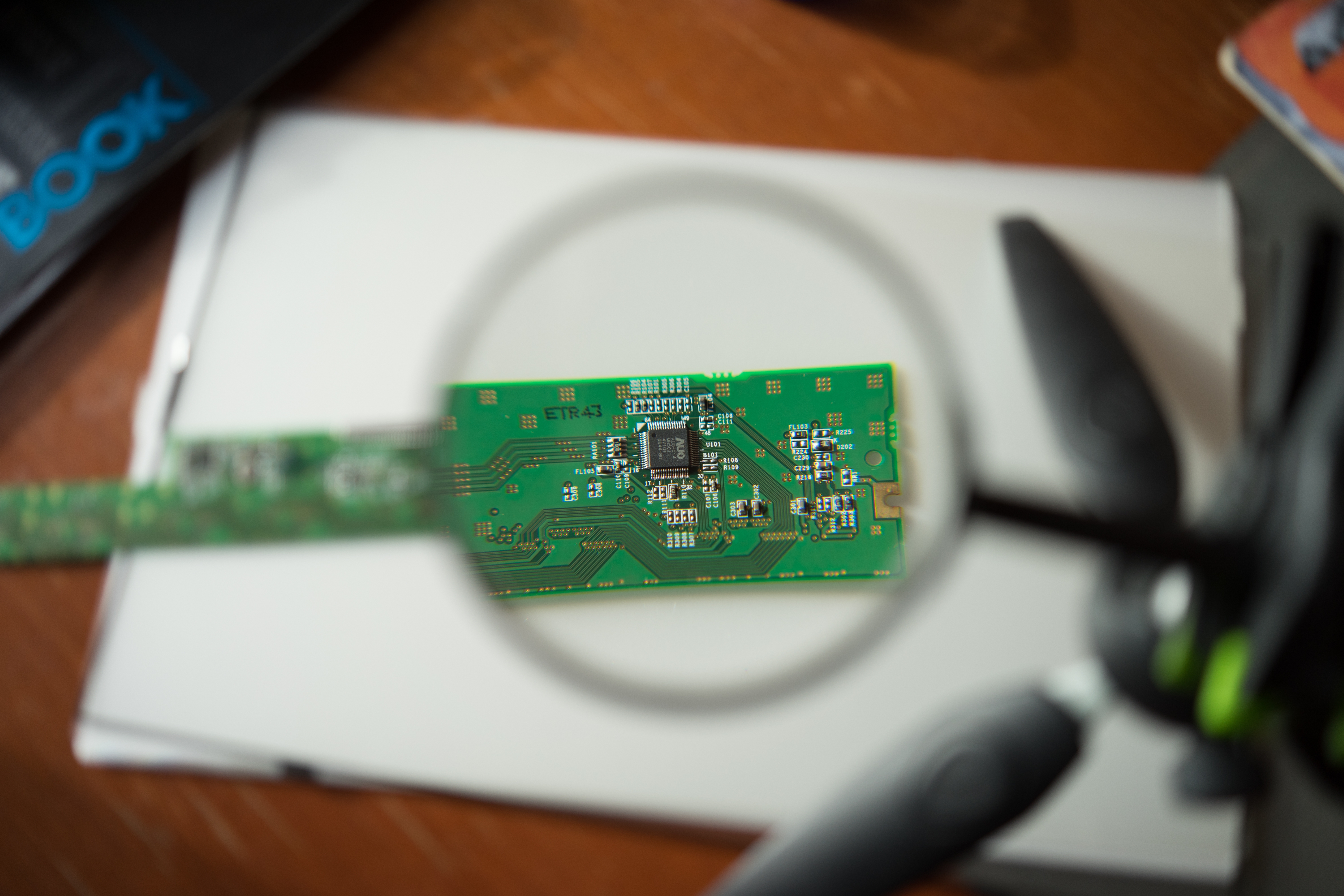
This course introduces learners to the full custom IC design flow including specification, schematic capture, layout, simulation, verification, and physical design. Participants will gain exposure to both analog and digital IC design techniques with a focus on CMOS technologies. The course emphasizes practical design using EDA tools like Cadence, Synopsys, or open-source platforms such as OpenROAD and Magic VLSI. Students will undertake a mini-project involving the design, layout, and verification of a simple IC block.
COURSE OBJECTIVE
Participants who complete this course will be able to :-
- Analyze and apply theoretical concepts of analog CMOS VLSI circuit design.
- Integrate and design analog CMOS VLSI circuits using innovative techniques.
- Evaluate CMOS circuit performance using industry-standard EDA tools.
- Understand the end-to-end process of IC design, from modeling to layout and verification.
LEARNING OUTCOME
Upon successful completion of the course, participants will be able to :-
- Explain core principles of analog CMOS VLSI circuit design.
- Design, simulate, and verify analog CMOS circuits using modern techniques.
- Apply circuit optimization strategies to meet performance and area constraints.
- Demonstrate proficiency in using EDA tools such as Virtuoso, Spectre, and Diva.
- Translate design concepts into working prototypes with verified performance.
SKILL AREAE
The course develops specialized skills in :-
- Analog and digital circuit design.
- Semiconductor device modeling (MOSFETs, diodes, current mirrors).
- EDA tools and simulation environments (Cadence, Virtuoso, Spectre).
- Layout design and verification (DRC, LVS, PEX).
- Problem-solving in high-performance circuit design.
- Innovation in application-specific IC development.
PREREQUISITE
- Academic : A minimum of diploma in Electronics, Electrical, or closely related discipline.
- Technical : Basic understanding of semiconductor physics, circuit theory, and logic design.
- Tools Familiarity : Exposure to simulation tools (e.g., SPICE) is advantageous but not mandatory.
TARGET AUDIENCE
- Diploma/Degree holders in Electronics/ Electrical/ Electronic & Communication Engineering.
- Professionals seeking specialization in VLSI/ASIC/SoC/FPGA domains.
- Research scholars pursuing advanced microelectronics or semiconductor studies.
CERTIFICATION
Participants who meet attendance, assessment, and project requirements will receive a Certificate of Completion in Custom IC Design.
DETAILS OF THE PROPOSED TRAINING
Introduction
The semiconductor industry is a vital sector within the electrical and electronics field, playing a crucial role in the advancement of modern technology. This industry is integral to various applications, including telecommunications, computing, automotive, and medical devices. The Custom IC Design aims to equip individuals with the necessary skills and knowledge to excel in the Custom IC Design domain.
Occupational Structure
The occupational structure within the semiconductor industry consists of various job levels, ranging from entry-level technicians to advanced IC design engineers. The primary job area covered in this program is Custom IC Design, which involves the design, simulation, and validation of integrated circuits. The structure includes the following levels:
- Assists in basic circuit layout, PCB design, and simple testing.
- Works under the supervision of senior engineers.
- Develops foundational knowledge in semiconductor devices and fabrication.
- Engages in circuit design and analysis with guidance from senior engineers.
- Gains experience with Electronic Design Automation (EDA) tools.
- Assists in debugging and verifying circuit performance.
- Conducts advanced IC design, simulation, and troubleshooting.
- Works on complex circuits, optimizing performance and power consumption.
- Coordinates with fabrication teams for manufacturing.
- Leads design projects and optimizes circuit performance.
- Works on advanced simulation techniques and verification processes.
- Provides mentorship to junior engineers.
- Oversees multiple design projects and ensures compliance with industry standards.
- Develops new methodologies for circuit design and verification.
- Manages collaboration between design, fabrication, and testing teams.
- Focuses on cutting-edge technology development in semiconductors.
- Engages in exploratory research for next-generation ICs.
- Works in collaboration with universities and research institutions.
Job Competencies
Professionals in this field must possess a strong understanding of MOS models, CMOS technologies, and circuit design principles. Key competencies include:
- MOSFET Knowledge: Understanding MOSFET operation, modeling techniques, and electrical characteristics.
- CMOS Circuit Design: Designing and analyzing CMOS circuits such as amplifiers, current mirrors, and voltage references.
- Fabrication Processes: Implementing semiconductor fabrication processes, including photolithography, doping, and etching.
- EDA Tools: Utilizing electronic design automation (EDA) tools for circuit simulation, layout, and verification.
- Compliance Standards: Ensuring compliance with industry standards such as IEEE, JEDEC, and ISO guidelines.
- Troubleshooting: Troubleshooting design issues and optimizing performance for power efficiency and stability.
Work Conditions
The work environment in the semiconductor industry varies depending on job roles. Common working conditions include :-
- Laboratory and cleanroom settings requiring adherence to strict safety and contamination protocols.
- Use of specialized software for circuit simulation, layout, and verification, such as Cadence Virtuoso and Synopsys tools.
- Collaboration with multidisciplinary teams, including design, process, and test engineers.
- Adherence to strict deadlines and project timelines to meet industry demands.
- Continuous learning to keep up with technological advancements and industry trends.
- High precision and accuracy in testing and fabrication to minimize defects and improve yield.
- Exposure to hazardous materials requiring proper safety measures, including the handling of chemicals used in semiconductor processing
Employment Prospects
The demand for skilled semiconductor professionals continues to grow due to the rapid expansion of the electronics, telecommunications, and computing industries. Employment opportunities exist in :-
- Semiconductor manufacturing companies, including major players like Intel, TSMC, and Samsung.
- Research and development institutions focusing on next-generation IC technologies.
- Telecommunications and consumer electronics industries developing cutting-edge devices.
- Automotive and medical device sectors requiring specialized semiconductor components.
- Academia and technical training institutions providing education and research opportunities.
- Startups and innovation centers working on emerging semiconductor applications.
Other position in semiconductor physical design engineering :
- IC Design Engineer.
- Physical Design Engineer.
- Senior IC Design Engineer.
- Senior Physical Design Engineer.
Course Topics
Chapter 1 – Introduction to MOS Models
- Fundamentals of MOSFET Operation and Characteristics
- Analytical Techniques for MOSFET Modeling
- Small-Signal Model Derivation and Application for MOS Transistors
- Comprehensive Modeling of Internal and External Parasitics
- Lab Exercise
Chapter 2 – CMOS Technologies and Layouts
- CMOS Technology Overview and Fabrication Process
- Detailed Physical Layout Techniques for MOS Transistors
- Verification Processes: DRC, PEX, and LVS
- Methods for Optimizing Silicon Utilization and Layout Efficiency
- Lab Exercise
Chapter 3 – CMOS Diodes and Active Resistors
- Overview of CMOS Diodes: Structure and Functionality
- Modeling and Analysis Techniques for CMOS Diodes and Active Resistors
- Design Trade-offs and Constraints
- Lab Exercise
Chapter 4 – CMOS Single-Stage Amplifiers
- Introduction to Single-Stage Amplifier Configurations
- Design and Analysis of Common-Source, Source Follower, and Common-Gate Amplifiers
- Loading Effects on Performance and Stability
- Performance Optimization in Single-Stage Amplifiers
- Lab Exercise
Chapter 5 – Basic and High Output Impedance Current Mirrors
- Principles of Current Mirror Circuits
- Design and Analysis of Widlar and Cascode Current Mirrors
- Impact on Amplifier Loading and Performance
- Trade-offs in High Output Impedance Mirror Designs
- Lab Exercise
Chapter 6 – CMOS Differential Pair and Cascode Amplifiers
- Introduction to Differential Pair and Cascode Amplifier Concepts
- Detailed Design and Analysis of Differential Amplifiers
- Implementation and Analysis using Current Mirrors
- Stability Compensation Techniques for Differential and Cascode Amplifiers
- Performance Trade-offs in Differential & Cascode Amplifiers
- Lab Exercise
Chapter 7 – CMOS Current, Output, and High-Gain Amplifiers
- Introduction to Current, Output, and High-Gain Amplifier Concepts
- Design and Performance Analysis of High-Gain CMOS Amplifiers
- Lab Exercise
Chapter 8 – CMOS Precision Voltage and Current Reference Circuits
- Introduction to Precision Voltage and Current Reference Circuits
- Design Principles and Analytical Methods
- Lab Exercise
Chapter 9 – Design and Compensation of CMOS Operational Amplifiers
- Introduction to Operational Amplifier Design Principles
- Pole-Zero Splitting and Compensation Techniques
- Design and Analytical Techniques for CMOS Op-Amps
- Lab Exercise